


Frequency Offset Adjustment – Frequency Deviation Caused by IC Internal Capacitance
1. Basic Information from Customer Feedback
| Customer Description | The customer reported that during product testing, the Bluetooth firmware download failed. |
Additional Information:
 | |
2. Processing Steps
2.1 Verification of the Defect:
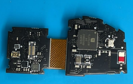
After receiving the customer’s PCB, tests were conducted. The test items included: IC input and output waveforms, on-board frequency, current (for the purpose of measuring DL), and negative resistance (|-R|).
Application Circuit Testing
Original crystal oscillator on PCBA: 2016/24MHz/12pF, external capacitors: C1=C2=20pF. Oscillation circuit test results are as follows:
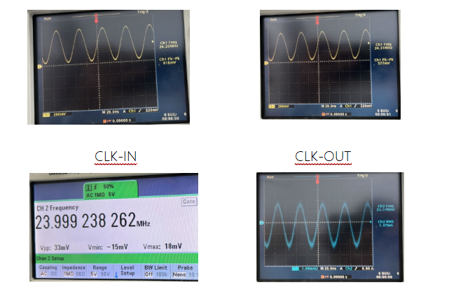
Oscillation circuit operating frequency FL = -31.8 ppm
Oscillation drive power: DL = 37.4μW (Reference value 300μW Max) Result: OK
Negative resistance characteristic: -R = 85Ω (Reference value |-R| > 180Ω) Result: NG
2.2 Abnormal Points
Judging from the test results, the on-board frequency offset (FL) is relatively large and the negative resistance is relatively small, with |-R| < 3RR.
2.3 Root Cause
This component is paired with the customer’s circuit board for Bluetooth function, which has high requirements for frequency offset. It is determined that the failure of Bluetooth firmware download is caused by FL exceeding the specification value.
2.4 Corrective Actions
After removing the external matching capacitors (set C1=C2=NC), the retest results are as follows:
Original crystal oscillator on PCBA: 2016/24MHz/12pF, matching capacitors removed: C1=C2=NC. Oscillation circuit test results are as follows:
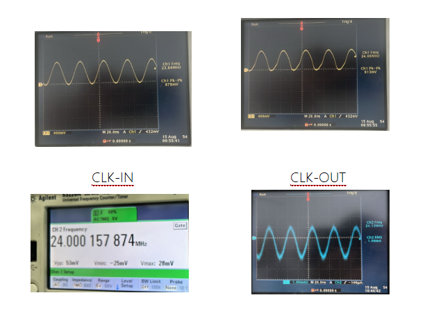
Oscillation circuit operating frequency FL = 6.5 ppm
Oscillation drive power: DL = 23.7μW (Reference value 300μW Max) Result: OK
Negative resistance characteristic: -R = 354Ω (Reference value |-R| > 180Ω) Result: OK
3. Final Disposal Measures
1. Judging from the test results, since the IC paired with the crystal oscillator on the customer’s circuit board has built-in capacitors, no additional external matching capacitors are required in practical applications. It is recommended that the customer adopt the matching scheme: C1=C2=NC.
2. Provide a matching test report and hold a meeting with the customer to explain the specific causes.

Contact
Official Chinese website:www.q-crystal.com.cn
Satisfaction quality, Just-in-time service, and Key-cost offering
©2026 SJK All Rights Reserved.