


Long trace length causes frequency offset-7050-25M-3.3V CMOS
1. Basic Information
| Customer Description | This is a new project of the customer. New samples of 7050-25M-3.3Vactive crystal oscillator were delivered. During reliability testing, frequency loss of lock occasionally occurred at the CPU end of the board. The issue was resolved after testing with crystal oscillators of the Taiwan brand TXC, and no similar defects were observed. |
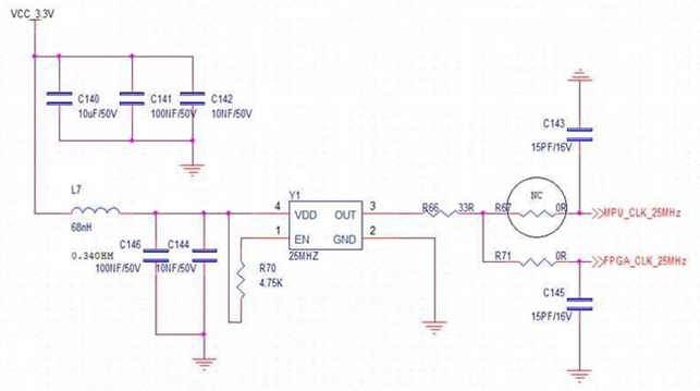
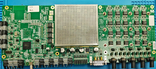
Supplementary Information 1. Original Circuit Parameters 2. Circuit Board View | |
2. Handling Procedures
2.1 Verify the Defect Phenomenon:
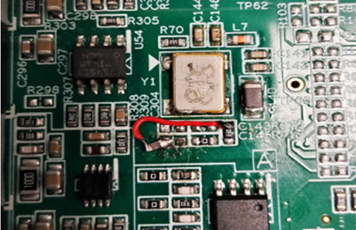
• a. Comparative testing shows that: When an oscilloscope probe touches the position of C145 on the circuit board with the SJK crystal oscillator, an instantaneous clock loss-of-lock phenomenon occurs in the backend chip (during loss-of-lock, the backend LED on the board turns OFF, and the test point TP58 = LOW).
• b. Cross-verification confirms that the loss-of-lock phenomenon is associated with the SJK crystal oscillator, indicating the root cause is the discrepancy between crystal oscillators.
2.2 Abnormal Analysis
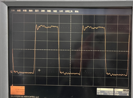
• a. The output waveforms of the crystal oscillator output pin, C145 and TP57 were measured separately with an oscilloscope, and no obvious abnormalities were observed.
• b. Meanwhile, a spectrum analyzer was used to detect the oscillation output frequency of the crystal oscillator via non-contact electromagnetic wave detection. The status of whether the crystal oscillator output frequency stopped oscillating or drifted during the abnormal (loss-of-lock) condition is shown in the figure below.
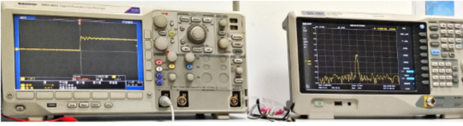
Test Result: No oscillation stop or frequency drift was observed in the crystal oscillator output.
• a. The anomaly was also eliminated by modifying the circuit in the following way: directly wiring the C145 of the defective board to the front end of the 33Ω resistor (R66).
• b. Standalone crystal oscillator test results (S&A 280, room temperature): All standalone crystal oscillator samples passed the test.
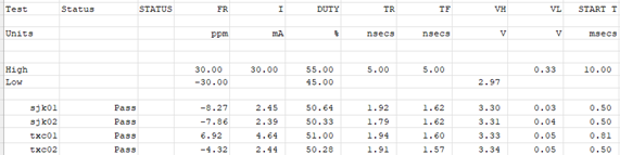
• c. Waveform data test (room temperature): PASS
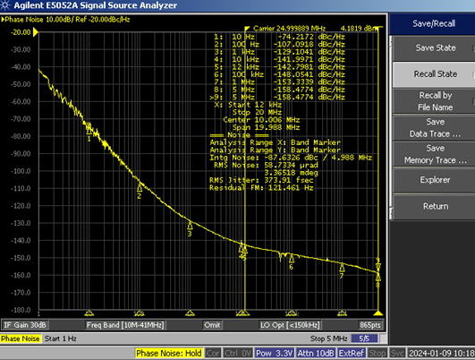
• d. The samples were further sent to a professional testing laboratory for jitter testing, and no abnormalities or significant discrepancies were found after comparison.
Qualified Product

Unqualified Product
• e. Internal Chip Comparison
The internal chip of the defective SJK sample is the frequency-stabilized chip from WinMEMS: LC5200
The internal chip of the qualified TXC sample is the NPC chip: NPC5027CX
2.3 Root Cause Analysis
a. Excessively Long PCBA Traces
The customer’s design includes a reserved circuit to drive two CPU main control chips. The traces from the crystal oscillator output terminal to the IC input terminal are excessively long and routed via two double-sided vias, resulting in significant circuit interference and high parasitic capacitance/inductance.
b. Drive Capability Discrepancy Caused by Different Crystal Oscillator Chips
2.4 Corrective Actions
a. Replace the internal driver chip of the crystal oscillator with the NPC chip featuring better drive capability, and deliver new samples for testing.
b. Recommend the customer optimize the active crystal oscillator output layout traces with the following guidelines:
• 1. Excessively long traces or repeated double-sided vias will cause a substantial increase in board parasitic capacitance as frequency rises. The common impedance formed by these parasitic components may amplify output noise. Therefore, traces should be minimized and repeated vias avoided.
• 2. For VDD and VSS power lines, a ground-loop noise reduction measure is recommended.
- 1. Unused leads should be eliminated as much as possible to minimize the impact of parasitic components and signal reflections.
- 2. Bypass capacitors should be placed directly adjacent to the oscillator IC between the power lines to reduce power supply noise. Ceramic chip capacitors are recommended as bypass capacitors.
3. Final Disposition
- 1. The customer revised the layout traces by following our recommendations.
- 2. New samples equipped with the NPC internal driver chip were provided to the customer for evaluation and testing, with passing results confirmed.

Contact
Official Chinese website:www.q-crystal.com.cn
Satisfaction quality, Just-in-time service, and Key-cost offering
©2026 SJK All Rights Reserved.