


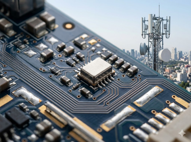
Optimizing 5G Base Station Performance with High-Frequency VCXOs
The transition to fifth-generation wireless networks demands unprecedented data throughput and ultra-low latency, putting immense pressure on the timing and synchronization architecture of network equipment. At the heart of this hardware ecosystem, engineers face the constant challenge of maintaining pristine signal integrity across highly complex transmission paths. This is exactly where a High-Frequency VCXO (Voltage-Controlled Crystal Oscillator) becomes an indispensable component in the RF signal chain. By providing a stable, electronically adjustable reference clock, it ensures that baseband units (BBU) and remote radio heads (RRH) operate in perfect harmony, preventing data packet loss and minimizing network desynchronization.
Navigating the Synchronization Demands of 5G Infrastructure
Designing a reliable 5G Base Station is not simply a matter of upgrading 4G LTE components to handle faster speeds; it requires a fundamental shift in how hardware processes time. Technologies like massive MIMO (Multiple-Input Multiple-Output), beamforming, and network slicing dictate strict time-error limits, frequently narrowing down to mere nanoseconds.
When hardware engineers evaluate the clocking tree for modern telecom equipment, they must address several severe operational demands:
- Fronthaul Synchronization:The CPRI and eCPRI interfaces connecting the BBU to the RRH require highly accurate clocking to prevent data frame slips. If the reference frequency drifts, the link simply drops.
- Carrier Aggregation Constraints:Combining multiple frequency bands demands synchronized sampling rates at the analog-to-digital (ADC) and digital-to-analog (DAC) converters.
- Thermal Shock Realities:Telecom towers and rooftop deployments expose hardware to rapid temperature fluctuations. The core oscillator must remain stable regardless of environmental stress.
To meet these demands, relying on standard passive quartz crystals paired with an external varactor diode is no longer sufficient. Integrated voltage-controlled solutions operating at elevated base frequencies are required to maintain system cohesion.
LVPECL Output: Handling High-Speed Data Rates
When designing the clocking distribution network for a 5G system, the choice of the oscillator's output logic format is just as critical as its operating frequency. As frequencies push past the 100 MHz threshold into the gigahertz realm, traditional single-ended CMOS outputs suffer from severe electromagnetic interference (EMI) and signal degradation due to parasitic capacitance on the PCB traces.
An LVPECL Oscillator (Low-Voltage Positive Emitter-Coupled Logic) is overwhelmingly the preferred choice for high-speed telecom applications. LVPECL utilizes a differential signaling approach, sending two complementary signals over a pair of traces. This differential nature inherently rejects common-mode noise, meaning any interference picked up along the board affects both traces equally and is cancelled out at the receiver. Furthermore, LVPECL logic provides a larger voltage swing and significantly faster rise and fall times compared to other differential standards.
To illustrate why engineers select specific logic outputs, consider the following technical comparison:
| Output Logic Type | Signaling Format | Voltage Swing (V) | Power Consumption | Best For... |
| CMOS | Single-ended | ~3.3V (Full rail) | Low | Low-frequency microcontrollers, <50 MHz |
| LVDS | Differential | ~0.35V | Medium | Low power, high-speed routing, up to 1.5 GHz |
| LVPECL | Differential | ~0.8V | High | Driving 5G timing ICs, ultra-low jitter, high frequencies |
Because 5G base stations require the absolute lowest jitter possible to drive the internal Phase-Locked Loops (PLLs), the slightly higher power consumption of LVPECL is a necessary and easily justified trade-off for the superior signal integrity it provides to the high-speed data converters.
Reducing Phase Noise and Jitter in Signal Chains
The most insidious threat to data integrity in any high-speed digital communication system is timing uncertainty. When dealing with gigabit-per-second transmission rates, even fractions of a picosecond of phase jitter can cause adjacent data bits to overlap, leading to a catastrophic increase in the system's Bit Error Rate (BER). In the RF signal chain of a cellular tower, phase noise directly degrades the Error Vector Magnitude (EVM) of the modulated signal. A poor EVM shrinks the signal-to-noise ratio margin, forcing the network to fall back to lower-order, slower modulation schemes like 64-QAM instead of the preferred 256-QAM or 1024-QAM. This fallback mechanism directly throttles the overall network throughput, frustrating end-users and reducing carrier efficiency. To counteract this, a modern High-Frequency VCXO utilizes fundamental mode inverted-mesa quartz blanks or highly optimized overtone designs. These specialized structural formations inherently possess a high Q-factor, which tightly confines the energy and drastically lowers the phase noise floor close to the carrier frequency. By integrating these low-noise crystal resonators with advanced low-noise ASIC-based oscillator circuits, hardware engineers can effectively clean up the clock signal before it is multiplied by the system's PLL. This pristine reference signal is what allows the subsequent transceivers to operate at their theoretical maximum efficiencies without being bottlenecked by thermal or flicker noise generated within the clock tree itself.
By ensuring the phase noise profile is exceptionally clean at offsets like 12 kHz to 20 MHz, engineers safeguard the entire transmission pipeline, guaranteeing that the high-frequency waves carrying user data remain crisp, distinct, and easily decodable by mobile devices.
Absolute Pulling Range (APR) Design Considerations
The defining characteristic of a VCXO is its ability to have its output frequency finely tuned via an analog control voltage input. This tuning capability allows the local oscillator to track an external reference clock, compensate for Doppler shifts, or adjust for the natural aging of the quartz crystal over its lifespan. However, when specifying these components, hardware engineers must carefully distinguish between the nominal Pulling Range and the Absolute Pulling Range (APR).
Designing a system based solely on the nominal pull range is a common and costly mistake. The APR guarantees the minimum amount of frequency deviation available specifically for tracking the input signal, after accounting for all internal oscillator errors. When calculating the necessary APR for telecom equipment, project engineers must factor in several distinct variables:
- Initial Tolerance:The frequency offset of the oscillator at room temperature immediately after manufacturing.
- Temperature Stability:How much the frequency drifts across the specified operating temperature range (e.g., -40°C to +85°C for industrial telecom).
- Power Supply Push:Slight frequency shifts caused by allowable fluctuations in the power supply voltage (VDD).
- Load Pull:Frequency variations induced by changes in the output load capacitance.
- Long-Term Aging:The natural shift in the quartz crystal's resonant frequency over 10 to 15 years of continuous operation.
To calculate the APR, you must subtract the sum of all these deviations from the total minimum pulling range. For example, if a high frequency oscillator has a total pull range of ±100 ppm, but the combined stability and aging errors total ±30 ppm, the guaranteed APR is ±70 ppm. Ensuring a wide enough APR guarantees that the phase-locked loop will never lose its lock, even as the base station hardware ages a decade into its deployment cycle.
Integrating Superior Timing for Future-Proof Networks
As telecom carriers continue to densify their networks and push into mmWave spectrums, the tolerance for timing errors will only continue to shrink. Upgrading the core synchronization hardware is no longer an optional enhancement; it is a fundamental requirement for 5G viability. Selecting the right frequency control components ensures the underlying architecture can handle tomorrow's data loads today.
For over 36 years, SJK has been at the forefront of frequency control innovation. As a leading manufacturer of premium quartz crystals and high-end oscillators, our automated production facilities deliver the precision components that power global telecommunications. Whether you require an ultra-low jitter LVPECL Oscillator, a custom-tuned VCXO, or enterprise-grade differential XOs, SJK provides the engineering expertise and reliable supply chain your next-generation B2B hardware projects demand. Partner with SJK today to secure the precise timing your 5G innovations require.
Frequently Asked Questions
What is the main difference between a standard XO and a VCXO?
A standard crystal oscillator (XO) outputs a fixed frequency based on its internal quartz resonator. A VCXO (Voltage-Controlled Crystal Oscillator) allows the user to subtly adjust the output frequency by varying a control voltage on a specific input pin. This is essential in telecom systems for tracking external reference signals and keeping equipment synchronized.
Why is an LVPECL Oscillator preferred for 5G Base Station designs?
An LVPECL Oscillator uses differential signaling with a wide voltage swing and extremely fast transition times. This makes it highly resistant to common-mode noise and electromagnetic interference, providing the ultra-low jitter necessary for driving high-speed data converters in a 5G Base Station.
How does Phase Jitter affect network performance?
Phase Jitter causes tiny timing fluctuations in the clock signal. In high-speed data transmission, this jitter can cause data bits to overlap, leading to misinterpretations by the receiver. This increases the bit error rate (BER) and degrades the Error Vector Magnitude (EVM), ultimately slowing down network data speeds.
What does Absolute Pulling Range (APR) mean in oscillator specifications?
Absolute Pulling Range (APR) is the usable frequency tuning range of a VCXO that remains available strictly for tracking an external signal, after subtracting all internal frequency errors. These errors include initial tolerance, temperature drift, voltage variations, and long-term crystal aging.
At what frequencies does a High-Frequency VCXO typically operate?
While traditional oscillators might operate below 50 MHz, a High-Frequency VCXO designed for telecommunications often operates between 100 MHz and 1 GHz or higher. These elevated base frequencies are generated using inverted-mesa quartz blanks or advanced multiplier circuits to minimize phase noise multiplication downstream.
Can a high frequency oscillator improve EVM in wireless transmitters?
Yes. By providing a clock signal with exceptionally low phase noise, a high frequency oscillator reduces the local oscillator (LO) noise introduced into the RF mixer. A cleaner LO signal directly improves the Error Vector Magnitude (EVM), allowing the transmitter to maintain high-density modulation schemes like 256-QAM for maximum data throughput.

Contact
Official Chinese website:www.q-crystal.com.cn
Satisfaction quality, Just-in-time service, and Key-cost offering
©2026 SJK All Rights Reserved.